


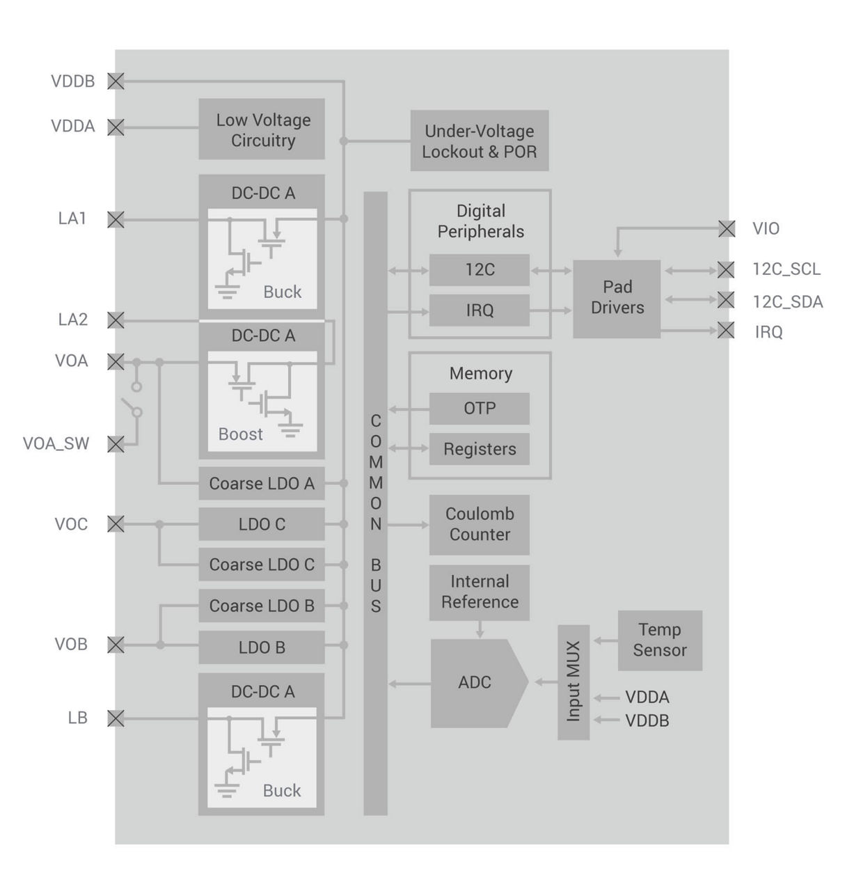
EFP01 PMIC Common Specs
Voltage Output A (VOA)
- Output Voltage: 1.7 V to 5.2 V
- DC-DC A can be configured in Buck/Boost, Buck-only, or Boost-only
- DC-DC A output be combined with the VOC linear regulator for more efficient regulation as the input voltage approaches the output voltage
- Firmware-programmable switched output (VOA_SW) allows complete powerdown of high leakage external circuitry in low power modes
Voltage Output B (VOB)
- Output Voltage:
- 0.8 V to 3.3 V (EFP0109/EFP0111)
- 0.8 V to 1.255 V (EFP0104/EFP0108)
- DC-DC B can be used only in Buck configuration
- Dedicated internal linear regulator in parallel provides more efficient regulation as the input voltage approaches the output voltage
Voltage Output C (VOC)
- Output Voltage: 1.7 V to 3.3 V
- Linear regulator only
- Can be used either to create an independent third output-supply or in conjunction with DC-DC A
Coulomb Counter
- Lossless (i.e. no sense resistor) measurement of charge into the load
Communication & Control
- Fully configurable I2C
- Direct Mode supports fast transitions between energymodes
- IRQ pin to notify host processor
Ultra-low Quiescent Current
- 150 nA with no outputs enabled
- 300 nA with a single output enabled
- +125 nA for each additional output enabled
Safety
- Programmable inrush current
- Short-circuit tolerant outputs
- Under-voltage lock-out (UVLO) circuitry holds device in lowest power reset state when VDDB is below 1.2 V
- Over-temperature monitoring and IRQ assertion
Wide Operating Range
- 0.8 V to 5.5 V input power supply
- -40 to 100 °C junction temperature
Package
- QFN20 3x3 mm
Find the Right EFP01 Device
Select Columns
| Part Number | Vdd Range (V) | Output Voltage Range (V) | DCDC A Configuration | Number of Output Voltage Rails | Lowest Quiescent Current (nA) | Coulomb Counting | I2C | Dig I/O Pins | DCDC B Output Voltage Range (V) | Temperature Range ºC | Package Type | Package Size (mm) |
|---|---|---|---|---|---|---|---|---|---|---|---|---|
| 1.8 5.5 | 1.7 3.3 | Wired Buck | 3 | 150 | 1 | 2 | 0.8 3.3 | -40 85 | QFN20 | 3 x 3 | ||
| 1.8 5.5 | 1.7 3.3 | Wired Buck | 3 | 150 | 1 | 2 | 0.8 1.26 | -40 85 | QFN20 | 3x3 | ||
| 1.8 5.5 | 1.7 3.3 | Buck with LDO | 2 | 150 | 1 | 2 | 0.8 3.3 | -40 85 | QFN20 | 3 x 3 | ||
| 1.8 5.5 | 1.7 3.3 | Buck with LDO | 2 | 150 | 1 | 2 | 0.8 1.26 | -40 85 | QFN20 | 3x3 | ||
| 1.8 5.5 | 1.7 3.3 | Buck/Boost | 3 | 150 | 1 | 2 | 0.8 3.3 | -40 85 | QFN20 | 3 x 3 | ||
| 0.8 5.5 | 1.7 3.3 | Buck/Boost | 3 | 150 | 1 | 2 | 0.8 1.26 | -40 85 | QFN20 | 3x3 | ||
| 0.8 1.8 | 1.7 3.3 | Single-Cell Boost | 3 | 150 | 1 | 2 | 0.8 1.26 | -40 85 | QFN20 | 3x3 | ||
| 1.8 3.6 | 1.7 3.3 | Wired Boost | 3 | 150 | 1 | 2 | 0.8 3.3 | -40 85 | QFN20 | 3x3 | ||
| 1.8 3.6 | 1.7 3.3 | Wired Boost | 3 | 150 | 1 | 2 | 0.8 1.26 | -40 85 | QFN20 | 3x3 | ||
| 1.5 5.5 | 1.7 5.2 | Boost Bootstrap | 3 | 150 | 1 | 2 | 0.8 3.3 | -40 85 | QFN20 | 3 x 3 |
Sort A -> Z
Sort Z -> A
Filter by values...
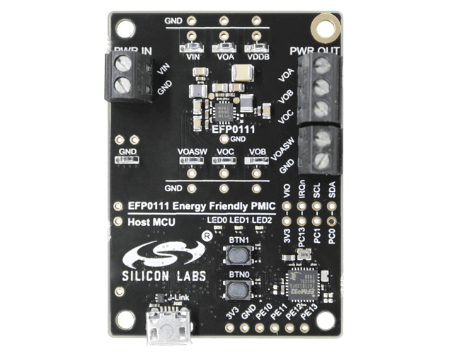
EFP0111 Single-Cell Boost Evaluation Kit
The EFP0111 Evaluation Kit is an excellent way to evaluate and characterize the EFP
PMIC in the Boost Bootstrap configuration.
EFP0111 Single-Cell Boost Evaluation Kit
The EFP0111 Evaluation Kit is an excellent way to evaluate and characterize the EFP
PMIC in the Boost Bootstrap configuration.
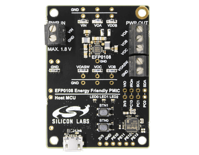
EFP0108 Single-Cell Boost Evaluation Kit
The EFP0108 evaluation kit is an excellent way to evaluate and characterize the EFP PMIC in the Single-Cell Boost configuration.
EFP0108 Single-Cell Boost Evaluation Kit
The EFP0108 evaluation kit is an excellent way to evaluate and characterize the EFP PMIC in the Single-Cell Boost configuration.
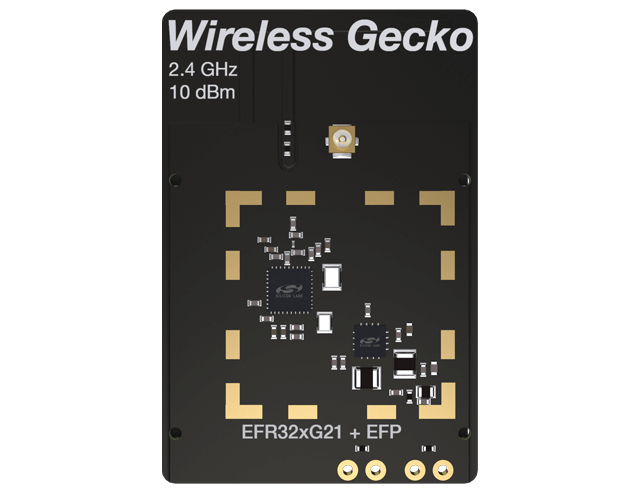
EFR32xG21 Wireless Gecko 2.4 GHz +10 dBm Radio Board with EFP (PMIC)
The Wireless Gecko SLWRB4179B radio board plugs into the mainboard provided with the Wireless Gecko Starter Kit. It is a complete reference design for evaluating EFR32xG21 Wireless SoCs with EFP in buck mode.
EFR32xG21 Wireless Gecko 2.4 GHz +10 dBm Radio Board with EFP (PMIC)
The Wireless Gecko SLWRB4179B radio board plugs into the mainboard provided with the Wireless Gecko Starter Kit. It is a complete reference design for evaluating EFR32xG21 Wireless SoCs with EFP in buck mode.