


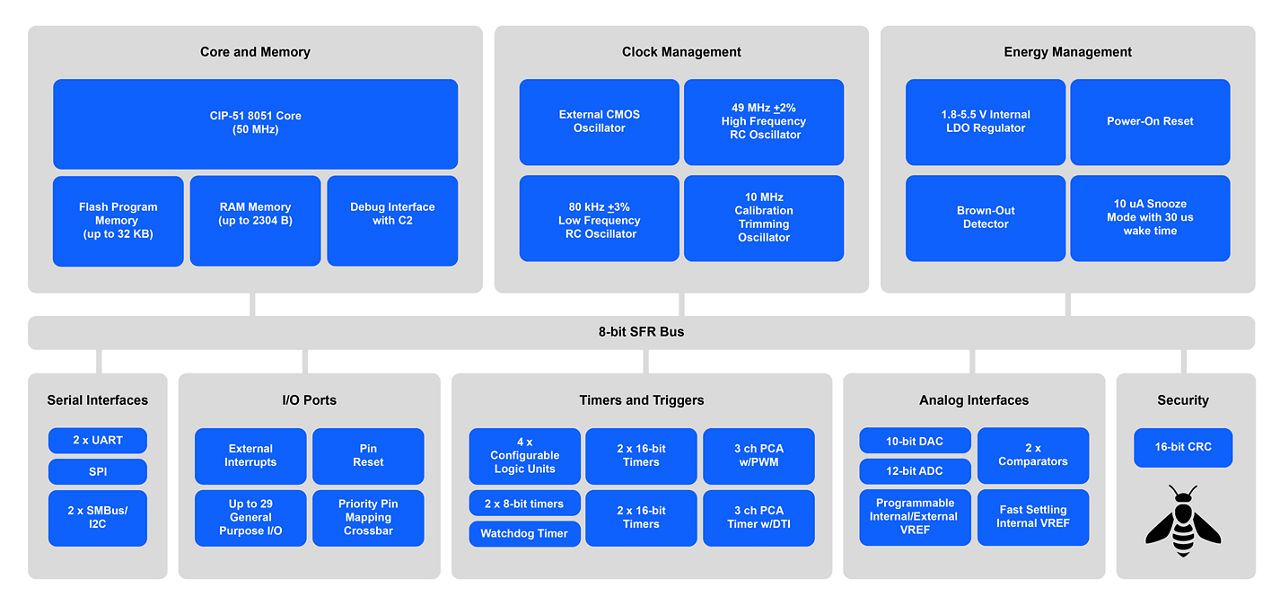
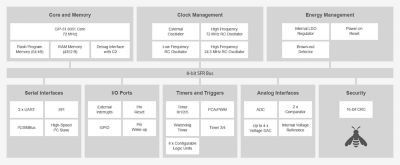
Introducing the EFM8BB5
Silicon Labs has announced the newest addition to the 8-bit portfolio, the EFM8BB5, which empowers developers with a versatile, highly integrated platform, ideal for transitioning from older 8-bit offerings. With compact package options as small as 2 mm x 2 mm and competitive pricing to cater to even the most budget-conscious designers, the BB5 family excels both as a means to augment existing products with simple functionality and as the primary MCU.


| Frequency | Flash (kB) | RAM (kB) | GPIO | ADC 1 | ADC 2 | DAC | ACMP | USB | SPI | UART | I2C | Packages | Timers | Vdd (Min) | Vdd (Max) | PWM/PCA Ch. | |
|---|---|---|---|---|---|---|---|---|---|---|---|---|---|---|---|---|---|
|
EFM8 BB5
EFM8 BB5 8-bit Microcontrollers (MCUs)
|
50 | 4, 8, 16, 32 | 0.5, 1.28, 2.30 | 9, 12, 16, 25, 29 | 12-bit, 12-ch., 12-bit, 16-ch, 12-bit, 16-ch., 12-bit, 5-ch., 12-bit, 8-ch. | — | -, 10-bit, 1-ch, 10-bit, 1-ch. | 0, 2 | 1 | 1, 2 | 1,2 | QFN12, QFN16, QFN20, QFN32, SOIC16, TSSOP20, TSSOP28 | 4 | 1.8 | 5.5 | 3 | |
|
EFM8 Busy Bee
EFM8 Busy Bee 8-bit Microcontrollers (MCUs)
|
25, 50 | 2, 4, 8, 16, 32, 64 | 0.25, 0.5, 2.25, 4.25 | 13, 16, 20, 22, 28, 29 | 12-bit, 12-ch., 12-bit, 15-ch., 12-bit, 20-ch. | — | 12-bit, 2-ch., 12-bit, 4-ch., — | 2 | 1 | 1, 2 | 1 1 | QFN20, QFN24, QFN28, QFN32, QFP32, SOIC16 | 4, 5, 6 | 2.2 | 3.6 | 3, 6 | |
|
EFM8 Laser Bee
EFM8 Analog Intensive Laser Bee 8-bit Microcontrollers (MCUs)
|
72 | 16, 32, 64 | 1.25, 2.25, 4.25 | 20, 28, 29 | 14-bit, 12-ch., 14-bit, 20-ch. | — | 12-bit, 2-ch., 12-bit, 4-ch., — | 2 | 1 | 2 | 1 1 | QFN24, QFN32, QFP32 | 6 | 2.2 | 3.6 | 6 | |
|
EFM8 Sleepy Bee
EFM8 Ultra Low Power Sleepy Bee 8-bit MCUs
|
25 | 2, 4, 8, 16, 32, 64 | 0.25, 0.5, 4 | 13, 16, 17, 24 | 10-bit, 15-ch., 10-bit, 23-ch., 12-bit, 10-ch., 12-bit, 9-ch. | — | — | 1, 2 | 1, 2 | 1 | 1 | CSP16, QFN20, QFN24, QFN32 | 4 | 1.8 | 3.6 | 3, 6 | |
|
EFM8 Universal Bee
EFM8 USB Capable Universal Bee 8-bit Microcontrollers (MCUs)
|
48 | 8, 16, 32, 64 | 2, 4 | 13, 22, 25, 40 | 10-bit, 20-ch., 10-bit, 32-ch., 12-bit, 11-ch., 12-bit, 20-ch. | — | — | 2 | 1 | 2 | 2 1 | QFN20, QFN28, QFN32, QFP48 | 5, 6 | 2.2, 2.7 | 3.8, 5.25 | 3, 5 | |
|
C8051F02x
Analog-Intensive MCUs
|
25 | 64 | 4.25 | 32, 64 | 10-bit, 8-ch., 100 ksps, 12-bit, 8-ch., 100 ksps | 8-bit, 8-ch., 500 ksps | 12-bit, 2-ch. | 2 | 1 | 2 | 1 | QFP100, QFP64 | 5 | 2.7 | 3.6 | 5 | |
|
C8051F04x
Analog-Intensive MCUs
|
25 | 32, 64 | 4.25 | 32, 64 | 10-bit, 13-ch., 100 ksps, 12-bit, 13-ch., 100 ksps | 8-bit, 8-ch., 500 ksps, — | 12-bit, 2-ch., — | 3 | 1 | 2 | 1 | QFP100, QFP64 | 5 | 2.7 | 3.6 | 6 | |
|
C8051F06x
Analog-Intensive MCUs
|
25 | 32, 64 | 4.25 | 24, 59 | 16-bit, 1-ch., 1 Msps | 16-bit, 1-ch., 1 Msps | 12-bit, 2-ch., — | 3 | 1 | 2 | 1 | QFP100, QFP64 | 5 | 2.7 | 3.6 | 6 | |
|
C8051F12x/13x
Analog-Intensive MCUs
|
50, 100 | 64, 128 | 8 | 32, 64 | 10-bit, 8-ch., 100 ksps, 12-bit, 8-ch., 100 ksps | 8-bit, 8-ch., 500 ksps, — | 12-bit, 2-ch., — | 2 | 1 | 2 | 1 | QFP100, QFP64 | 5 | 2.7 | 3.6 | 6 | |
|
C8051F30x
Small Form Factor Microcontrollers
|
25 | 2, 4, 8 | 0.25 | 8 | 8-bit, 8-ch., 500 ksps, — | — | — | 1 | 0 | 1 | 1 | QFN11 | 3 | 2.7 | 3.6 | 3 | |
|
C8051F31x
Small Form Factor Microcontrollers
|
25 | 8, 16 | 1.25 | 21, 25 | 10-bit, 13-ch.,200 ksps, 10-bit, 17-ch., 200 ksps, — | — | — | 2 | 1 | 1 | 1 | QFN24, QFN28 | 4 | 2.7 | 3.6 | 5 | |
|
C8051F32x/34x
USB Microcontrollers
|
25, 50 | 16, 32, 64 | 1.5, 2.25, 4.25 | 15, 21, 25, 40 | 10-bit, 13-ch., 200 ksps, 10-bit, 20-ch., 200 ksps, 10-bit, 21-ch., 200 ksps, — | — | — | 0, 2 | 0, 1 | 1, 2 | 1 | QFN28, QFN32, QFP48 | 2, 4 | 2.7, 4 | 5.25 | 0, 5 | |
|
C8051F33x
Small Form Factor Microcontrollers
|
25 | 2, 4, 8, 16 | 0.75 | 17, 21 | 10-bit, 16-ch., 200 ksps, — | — | 10-bit, 1-ch., — | 1 | 1 | 1 | 1 | QFN20, QFN24 | 4 | 2.7 | 3.6 | 3 | |
|
C8051F35x
Analog-Intensive MCUs
|
50 | 8 | 0.75 | 17 | 16-bit, 8-ch., 1 ksps, 24-bit, 8-ch., 1 ksps | — | 8-bit, 2-ch. | 1 | 1 | 1 | 1 | QFN28 | 4 | 2.7 | 3.6 | 3 | |
|
C8051F36x
C8051F36x Small Form Factor Microcontrollers
|
100 | 32 | 1.25 | 25, 39 | 10-bit, 17-ch., 200 ksps, 10-bit, 21-ch., 200 ksps | — | 10-bit, 1-ch. | 2 | 1 | 1 | 1 | QFN28, QFP48 | 4 | 2.7 | 3.6 | 6 | |
|
C8051F38x
USB Microcontrollers
|
50 | 16, 32, 64 | 2.25, 4.25 | 25, 40 | 10-bit, 21-ch., 500 ksps, 10-bit, 32-ch., 500 ksps, — | — | — | 2 | 1 | 2 | 2 | QFN32, QFP48 | 6 | 2.7 | 5.25 | 5 | |
|
C8051F39x
Small Form Factor Microcontrollers
|
50 | 4, 8, 16 | 1 | 17, 21 | 10-bit, 16-ch., 500 ksps, — | — | 10-bit, 2-ch., — | 1 | 1 | 1 | 2 | QFN20, QFN24 | 6 | 1.8 | 3.6 | 3 | |
|
C8051F41x
Small Form Factor Microcontrollers
|
50 | 16, 32 | 2.25 | 20 | — | — | 12-bit, 2-ch. | 2 | 1 | 1 | 1 | QFN28 | 4 | 2 | 5.25 | 6 | |
|
C8051F50x
Automotive & Industrial MCUs
|
50 | 32, 64 | 4.25 | 25, 33, 40 | 12-bit, 25-ch., 200 ksps, 12-bit, 32-ch., 200 ksps | — | — | 2 | 1 | 1 | 1 | QFN32, QFN40, QFN48, QFP48 | 4 | 1.8 | 5.25 | 6 | |
|
C8051F51x
Automotive & Industrial MCUs
|
50 | 32 | 4.25 | 33 | 12-bit, 32-ch., 200 ksps | — | — | 2 | 1 | 1 | 1 | QFN40 | 4 | 1.8 | 5.25 | 6 | |
|
C8051F52x
Automotive & Industrial MCUs
|
25 | 2 | 0.25 | — | 12-bit, 6-ch, 200 ksps | — | — | — | — | — | — | DFN10 | — | 2 | 5.25 | — | |
|
C8051F53x
Automotive & Industrial MCUs
|
25 | 4, 8 | 0.25 | 16 | 12-bit, 16-ch., 200 ksps | — | — | 1 | 1 | 1 | QFN20, TSSOP20 | 3 | 2 | 5.25 | 3 | ||
|
C8051F54x
Automotive & Industrial MCUs
|
50 | 8, 16 | 1.25 | 18, 25 | 12-bit, 18-ch., 200 ksps, 12-bit, 25-ch., 200 ksps | — | — | 2 | 1 | 1 | QFN24, QFN32 | 4 | 1.8 | 5.25 | 6 | ||
|
C8051F55x
Automotive & Industrial MCUs
|
50 | 16, 32 | 2.25 | 18 | 12-bit, 18-ch., 200 ksps | — | — | 2 | 1 | 1 | 1 | QFN24 | 4 | 1.8 | 5.25 | 6 | |
|
C8051F56x
Automotive & Industrial MCUs
|
50 | 32 | 2.25 | 25, 33 | 12-bit, 25-ch., 200 ksps, 12-bit, 32-ch., 200 ksps | — | — | 2 | 1 | 1 | 1 | QFN32, QFN40 | 4 | 1.8 | 5.25 | 6 | |
|
C8051F57x
Automotive & Industrial MCUs
|
50 | 32 | 2.25 | 33 | 12-bit, 32-ch., 200 ksps | — | — | 2 | 1 | 1 | 1 | QFN40 | 4 | 1.8 | 5.25 | 6 | |
|
C8051F58x
Automotive & Industrial MCUs
|
50 | 96, 128 | 8 | 25, 40 | 12-bit, 25-ch., 200 ksps, 12-bit, 32-ch., 200 ksps | — | — | 3 | 1 | 2 | 1 | QFN32, QFN48, QFP48 | 6 | 1.8 | 5.25 | 12 | |
|
C8051F92x-93x
Ultra Low-Power MCUs
|
25 | 32, 64 | 4.25 | 16, 24 | 10-bit, 15-ch., 300 ksps, 10-bit, 23-ch., 300 ksps | — | — | 2 | 2 | 1 | 1 | QFN24, QFN32 | 4 | 0.9 | 3.6 | 6 |
Featured 8-bit MCU Kits
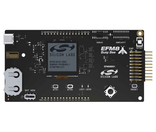
EFM8BB51 8-bit MCU Explorer Kit
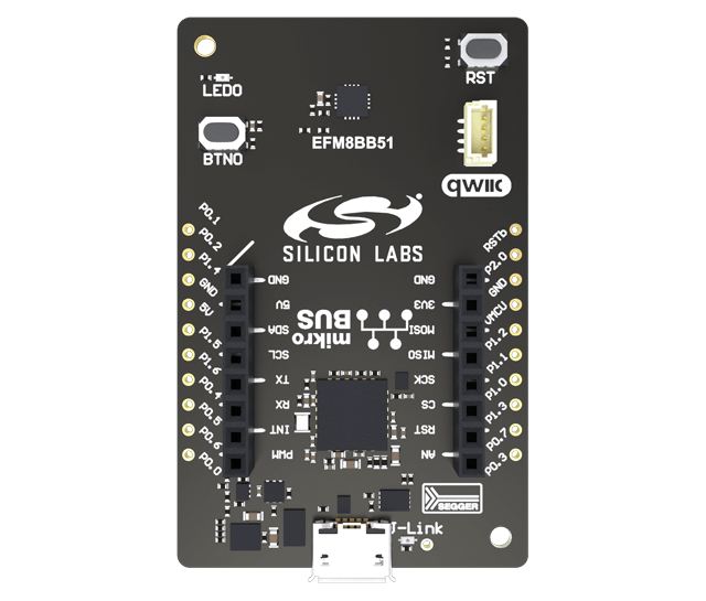
EFM8BB51 8-bit MCU Explorer Kit
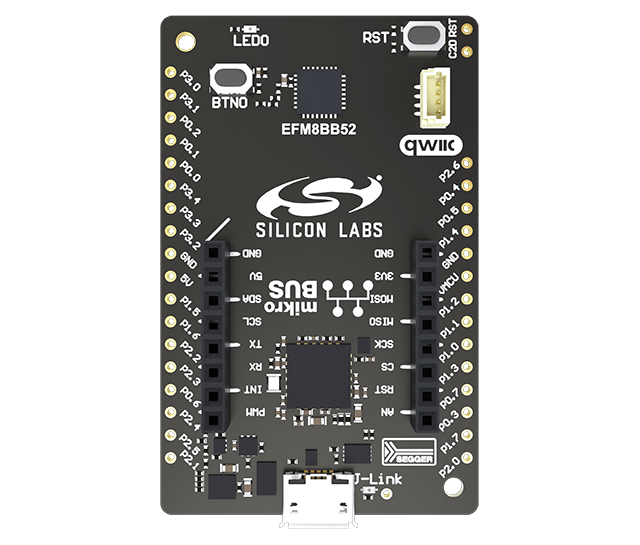
EFM8BB52 8-bit MCU Pro Kit
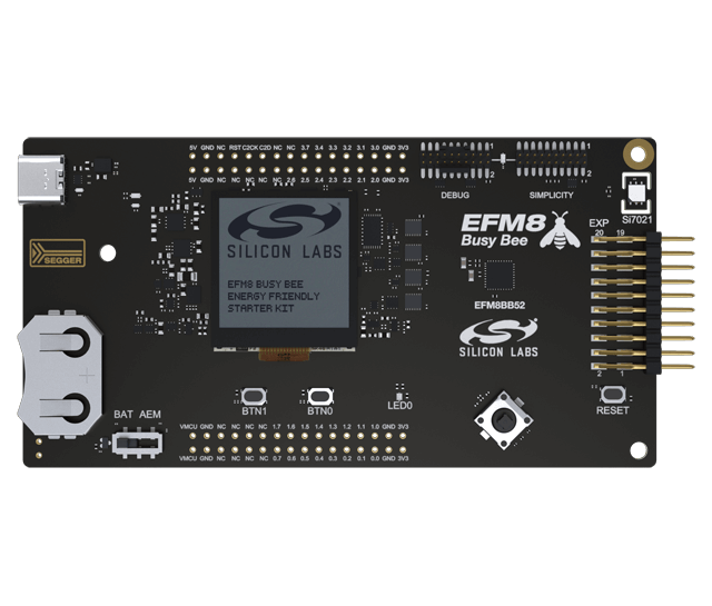
EFM8BB52 8-bit MCU Pro Kit
EFM8BB51 8-bit MCU Pro Kit
EFM8BB51 8-bit MCU Pro Kit
EFM8BB52 8-bit MCU Explorer Kit
EFM8BB52 8-bit MCU Explorer Kit
EFM8 BB50 8-bit MCU Explorer Kit
EFM8 BB50 8-bit MCU Explorer Kit
EFM8 BB50 8-bit MCU Pro Kit
EFM8 BB50 8-bit MCU Pro Kit
8-bit USB Debug Adapter
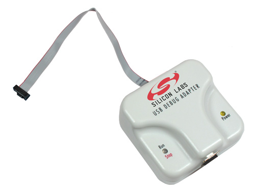
8-bit USB Debug Adapter
Simplicity Link Debugger
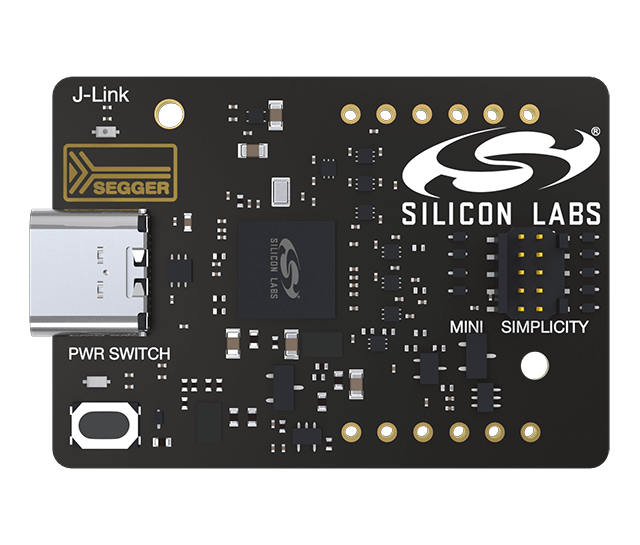
Simplicity Link Debugger
8-bit Software Development
Simplicity Studio is the core development environment designed to support the Silicon Labs IoT portfolio of 8-bit SoCs. It provides access to target device-specific web and SDK resources in the Launcher; software and hardware configuration tools; an integrated development environment (IDE) featuring industry-standard code editors, compilers and debuggers; and advanced, value-add tools for network analysis and code-correlated energy profiling.
Silicon Labs offers an advanced 8-bit microcontroller studio, available at no charge to developers. These tools unlock the power and flexibility of the 8-bit 8051 microcontroller family. All C8051Fxxx families are supported by the 8-bit Studio. If your 8051 device does not appear in the 8-bit studio list, you can also use Simplicity Studio Software Suite.
Simplicity Studio
Making development easier and more efficient by providing everything needed - from initial concept to final product.
32-bit MCU SDK
This software package provides all of the drivers and services needed for a successful 32-bit MCU project.
Precision32 32-bit MCU Development Suite
This tool unlocks the power and flexibility of the Precision32™ 32-bit microcontroller family.
Find the Right 8-bit Microcontroller for your Application
Featured 8-bit Microcontroller Resources

